USB laser switch
Carrier board and case mockup
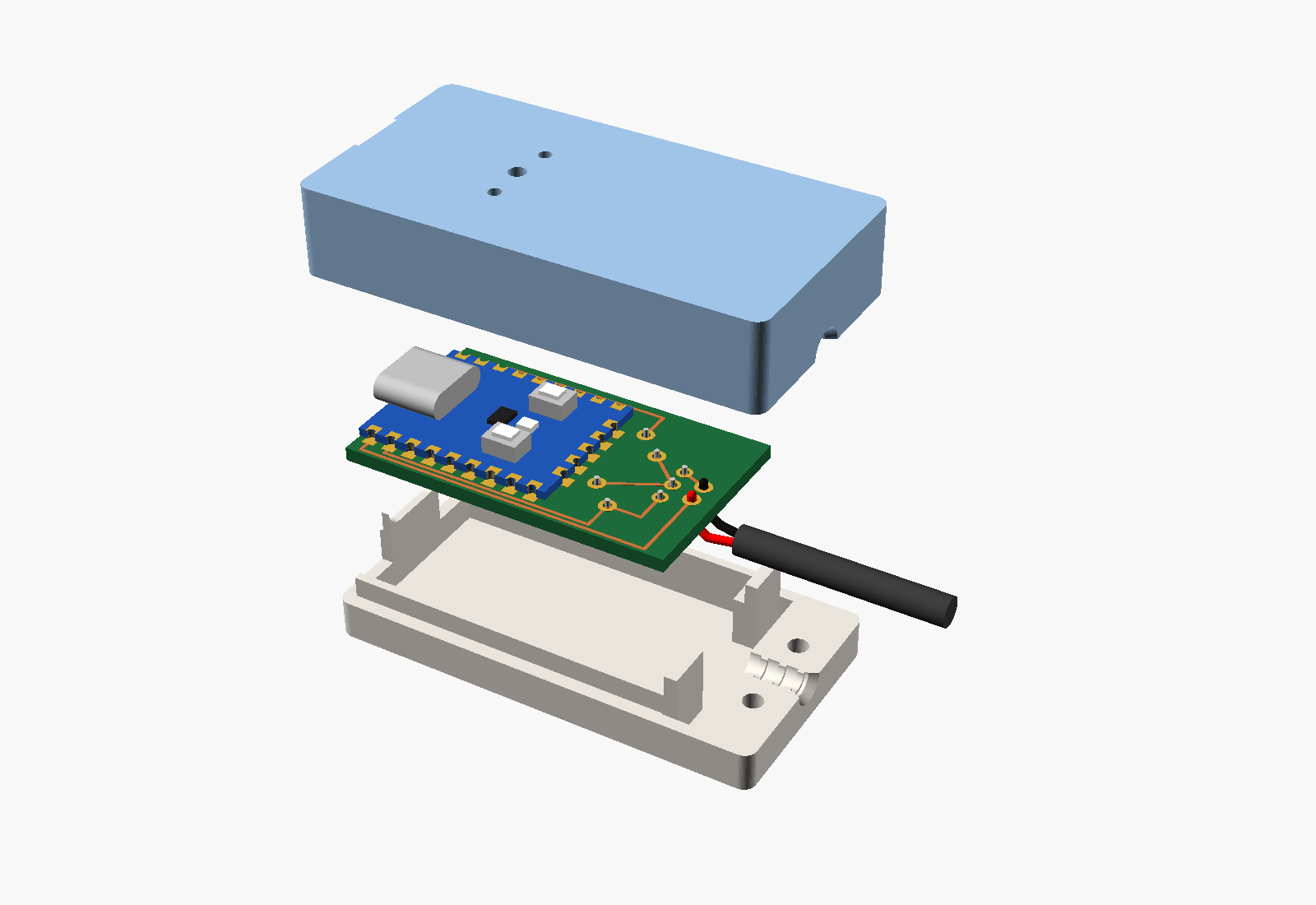
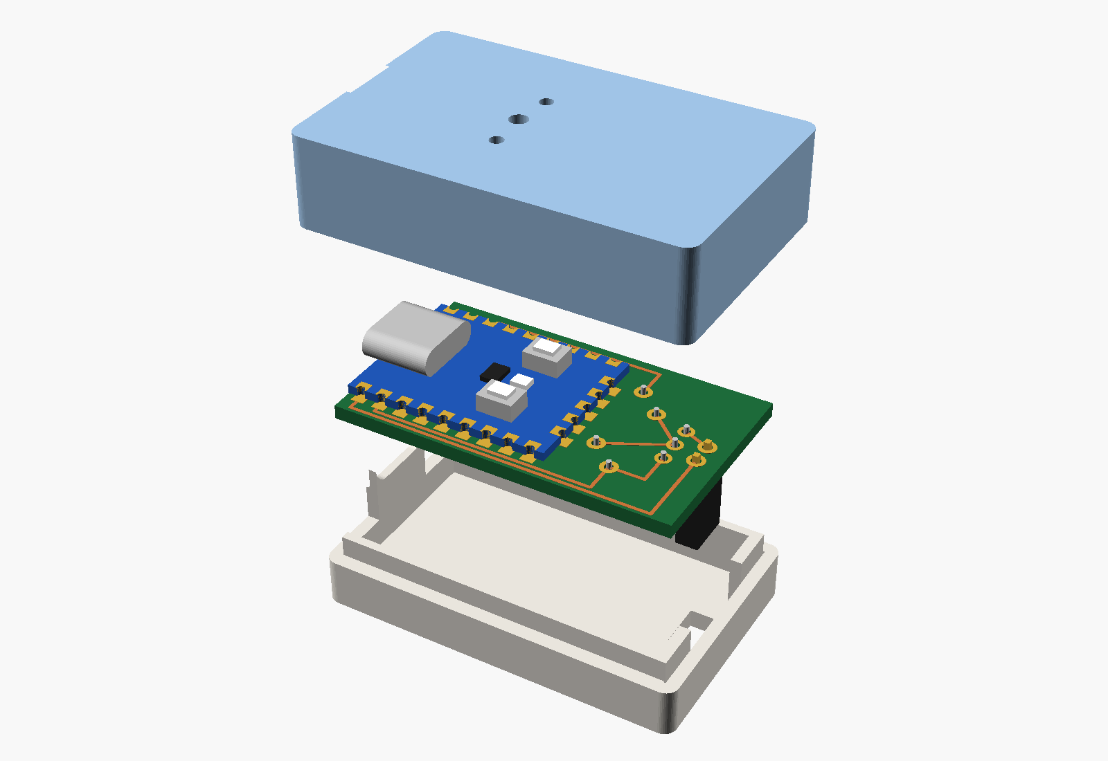
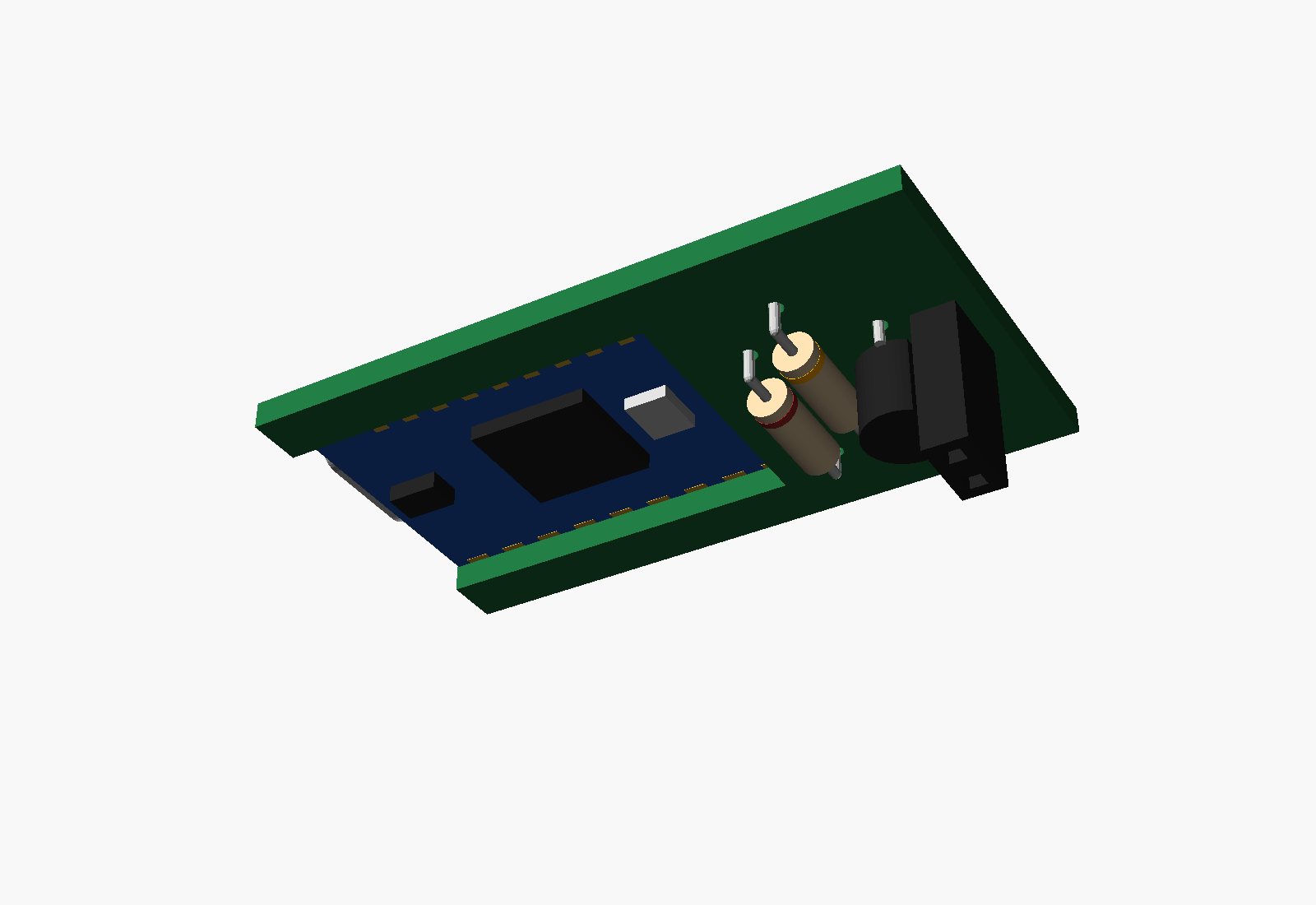
A parametric OpenSCAD model of the whole assembly: the RP2040-Zero, a single-sided through-hole carrier board that holds the module and the laser switch circuit (circuit.md), and a two-piece printed case in two versions.
- Model: cad/usb_power_switch.scad. Every dimension is a named parameter at the top of the file.
just renderwrites preview images tocad/renders/.just stlwrites printable STLs tocad/stl/. The lids are already flipped upside down for printing.just viewerbuilds interactive 3D views, where each part can be turned on, ghosted or hidden: cable version, Molex version.
| Molex version | Cable version | |
|---|---|---|
| Laser connection | Vertical 2-pin 0.1” female header. It hangs under the board and plugs in from the bottom of the case | AM2464 cable (2 × 20 AWG, 3.4 mm) soldered into the board |
| Closing the case | Glue | 2 × M2×8 self-tapping screws, put in from the bottom through the cable clamp |
| Outside size (L × W × H) | 42.6 × 26.6 × 15.65 mm | 52.1 × 26.6 × 14.65 mm |
RP2040-Zero (as modelled)
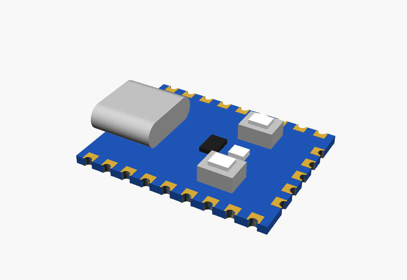
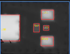
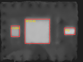
The part positions come from a 3D scan of the module (scan/rp2040-zero-scan.stl). The scan has two patches, the top and the bottom. Each was laid flat and turned into a height map, and the raised parts were measured from those maps.
| Top-side model outlines on the scan | Bottom-side model outlines on the scan |
|---|---|
 |
 |
- Board 23.5 × 18 × 1.0 mm. The scan measures 23.53 × 18.18, matching Waveshare’s drawing.
- Castellations at 2.54 mm pitch: 9 on each long side, 5 on the end opposite the USB. Long side: 5V, GND, 3V3, GP29, GP28, GP27, GP26, GP15, GP14 (starting at the USB end). Other long side: GP0–GP8. End: GP9–GP13. The scan is too coarse to show the half-holes, so the model assumes each row is centered along its edge.
-
Top side (x from the USB end, y from the centerline):
Part Center (x, y) Size Height above board USB-C runs from 1.25 past the edge back to x = 6.7, centered 8.94 wide 3.15 BOOT button (5V side) 16.0, −4.6 4.2 × 3.2 2.5 RESET button (GP0 side) 16.1, +4.45 4.2 × 3.2 2.5 RGB LED 15.65, 0 1.9 × 1.6 0.7 Flash chip 12.4, 0 2.0 × 2.9 0.56 The two buttons sit side by side at the same distance from the USB, with the LED between them. The USB-C is the tallest part on top, 0.65 mm taller than the buttons.
- Bottom side: RP2040 (7.3 × 7.3 × 0.92, center 12.55 from the USB end), crystal (2.6 × 3.3 × 0.76, at 19.0), and voltage regulator (3.1 × 2.1 × 1.05, at 3.05). The underside parts stand up to 1.05 mm, not 0.5. They all sit inside the carrier’s cutout, which is 1.6 mm deep, so this doesn’t change the carrier.
Carrier board
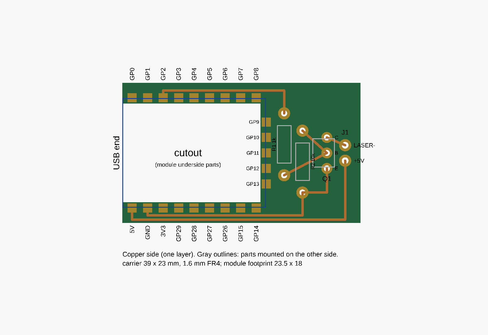
Single-sided, through-hole. 39 × 23 mm, 1.6 mm FR4, copper on one side only.
- Which side is which. The module solders to the copper side, so the through-hole parts go on the plain side. Their leads push up through the board and are soldered on the copper side, next to the module. Every solder joint is on the same side.
- Module footprint. Pads for all 23 castellations, even though only 5V, GND and GP2 are used; the rest hold the module down. Each pad runs 0.7 mm under the module edge and 0.8 mm past it for the solder fillet.
- Cutout. Inside the 0.9 mm pad band, the board is cut away so the module’s underside parts have room. The cutout runs out through the USB end of the carrier. The module therefore sits flat on the pads.
- Routing on one layer, with no crossings. 5V and GND both leave the module on the same side and run side by side to the back, outside the pad row: 5V in the outer lane, GND in the inner one. GP2 runs down the other side. That’s why the board is 2.5 mm wider than the module on each side. Traces are 0.4 mm, with at least 0.25 mm clearance.
- Through-hole pads are 2.0 mm across with 1.0 mm holes. They’re bigger than usual because the holes on a single-sided board aren’t plated.
| Ref | Part | Mounting |
|---|---|---|
| R1 | 1 kΩ, 1/4 W axial | Lying flat, 10.16 mm (0.4”) hole spacing |
| R2 | 10 kΩ, 1/4 W axial | Lying flat, 10.16 mm hole spacing |
| Q1 | 2N3904 or PN2222A, TO-92 | Standing, legs spread to 2.54 mm, order E-B-C |
| J1 | 2-pin 0.1” vertical female header (Molex version) or the two cable wires | 1.1 mm holes, 2.54 mm apart. Pin 1 = +5V, pin 2 = LASER− |
Check Q1’s pinout. 2N3904 and PN2222A in TO-92 are E-B-C, reading left to right with the flat face toward you and the legs down. Some parts sold as “2N2222” in TO-92 are C-B-E, which would fit the board backwards.
Build order
- Put R1, R2 and Q1 in from the plain side (and the header, for the Molex version). Bend the leads over a little so the parts stay put.
- Turn the board copper side up. Solder and trim the leads.
- Set the module on its pads, lined up with the USB end of the carrier, and solder the castellations.
- Cable version: push the two wires up through J1 from the plain side and solder them on the copper side.
You turn the board over once, after step 1, and do all the soldering from then on without turning it again.
Case
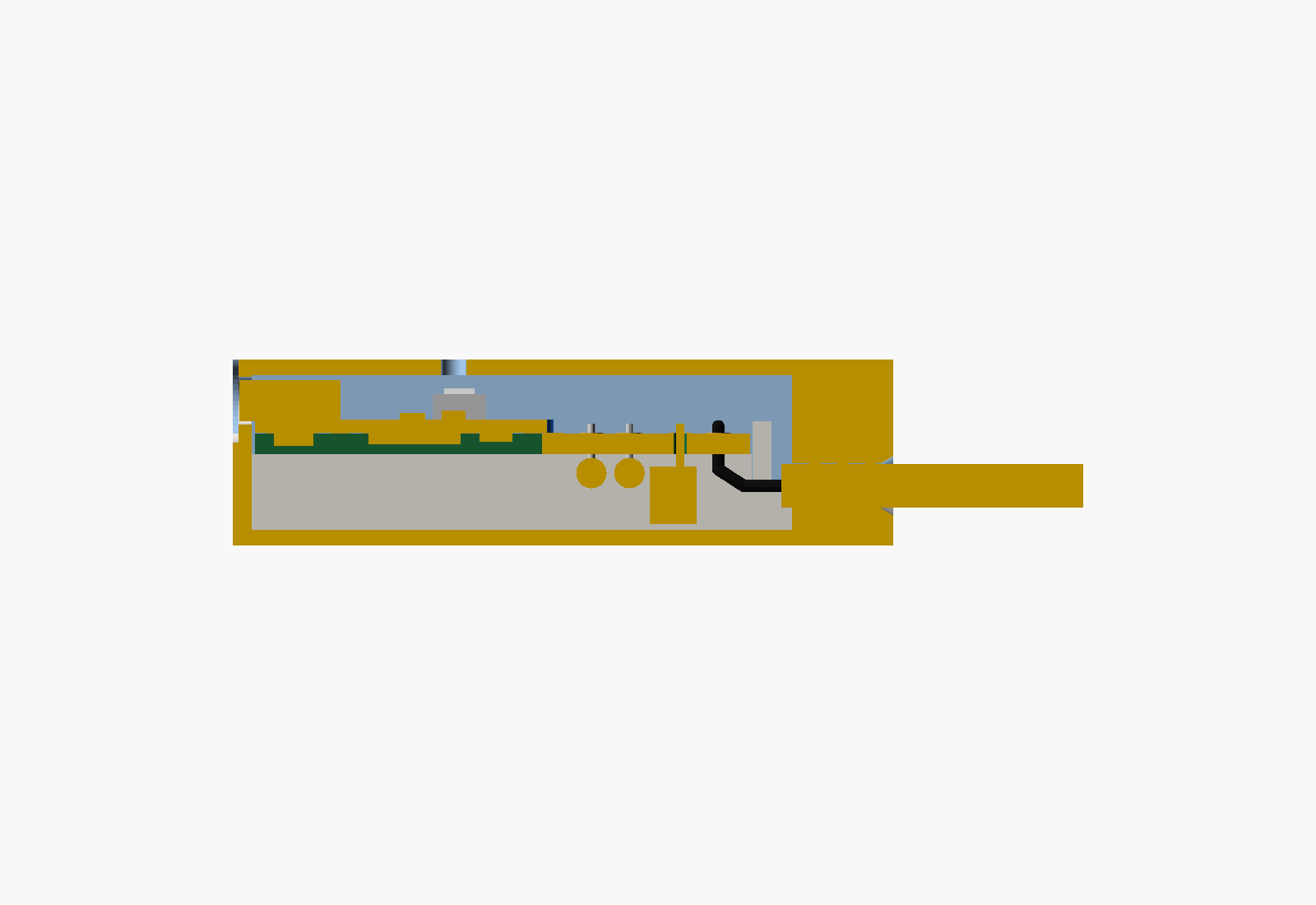
Section through the middle (cut surfaces shown in gold). Left to right: USB opening, module on the carrier, R1 and R2 under the board, Q1 standing, the wires coming up into J1, and the cable clamp.
- Two halves. They meet at a flat plane 2.5 mm below the carrier, through the middle of the cable, so each half clamps half of it. Under the USB opening, a tab on the bottom half rises to the middle of the receptacle. That lets the lid come straight down over the USB-C, which sticks out into the front wall.
- Depth. 6 mm of room under the carrier for the standing TO-92 (about 5.5 mm). This is what sets the overall height.
- Walls 1.5 mm, floor and lid 1.2 mm. 0.3 mm clearance around the carrier.
- Carrier support. Rails along both sides and at the back corners hold the carrier up. They stand 2.5 mm above the split, which locates the lid. The middle of the back is left open for the cable’s wires. Two posts in the lid press down on the carrier’s back corners.
- Back stops (cable version). Behind the carrier there is a 3 mm gap where the wires turn up into J1. Two posts at the back corners close it off: they rise from the floor to 1 mm above the top of the carrier, 0.2 mm behind its back edge, so the board can’t slide back. They sit at |y| ≥ 6 mm, clear of the wires and the clamp screws. The front wall and the USB-C in its slot stop the board moving forward. The Molex version’s back wall is only 0.3 mm behind the board, so it needs no stops.
- USB opening: 9.4 × 3.8 mm, rounded to match the receptacle, with a 12 × 6.6 mm recess 0.5 mm deep around it. The receptacle face ends up 0.55 mm behind the case surface, so the plug seats fully.
- Lid holes: a 2 mm window over the RGB LED, and 1.5 mm pinholes over BOOT and RESET (for a paperclip).
- Molex version: the floor is 2.2 mm thick, so the bottom of the case is flat. The header comes out through a hole in the floor and stands 0.3 mm above it, so the mating plug seats fully. A raised box under the floor would have had to print in mid-air.
- Cable version: a clamp block 8 mm long at the back end. The channel is 3.5 mm across, with three ridges that narrow it to 2.7 mm and bite into the 3.4 mm jacket. Two M2×8 self-tapping screws go up from the bottom: the heads sit in 4.2 mm counterbores, and the screws bite into 1.7 mm pilot holes in the lid.
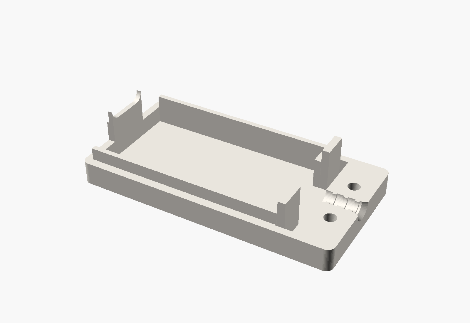
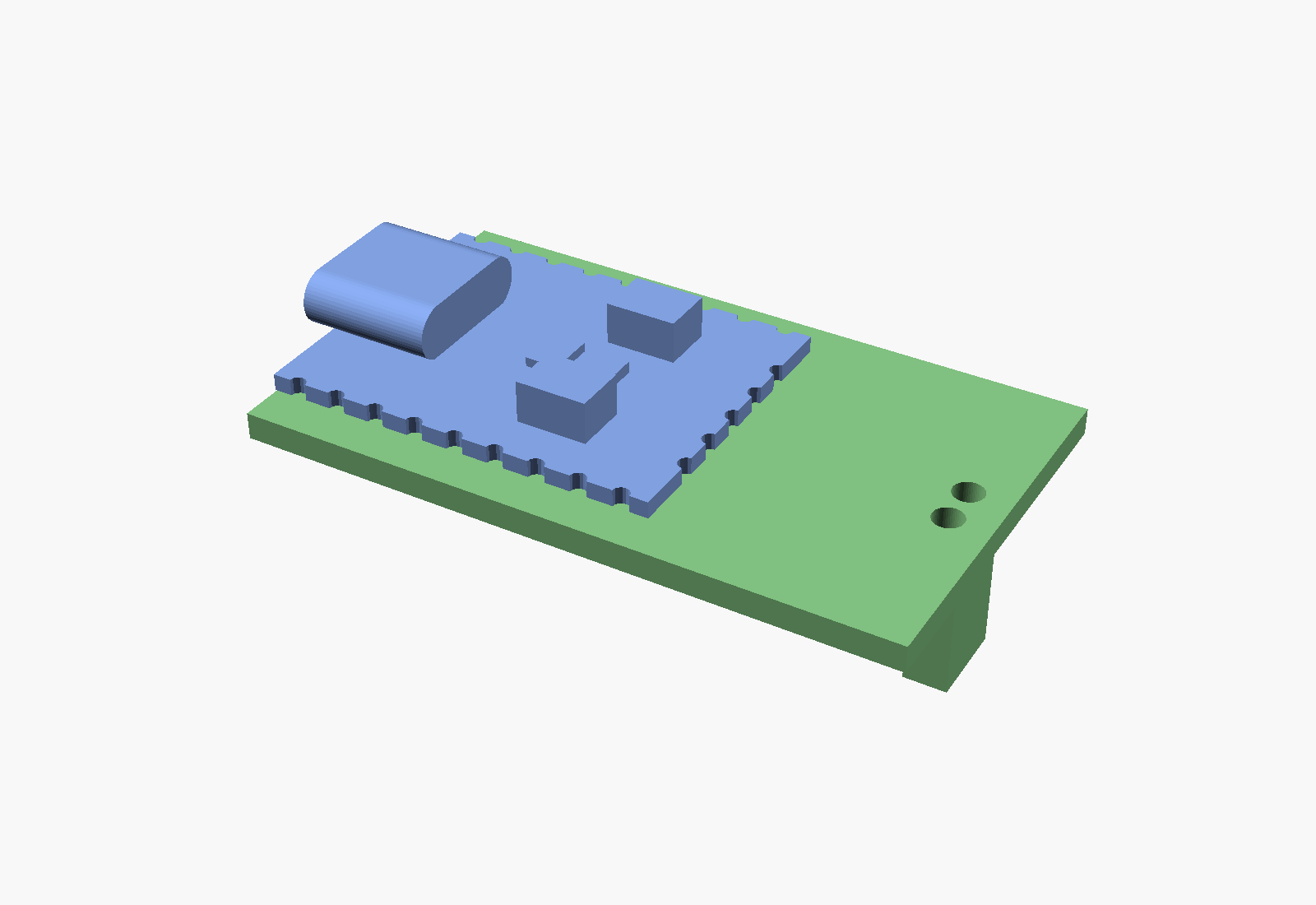
Fit-test mockups
just stl also writes two printable stand-ins for testing the case
before the real board exists:
carrier_mock_cable.stl,carrier_mock_molex.stl: the carrier plate with its cutout, plus solid blocks where R1, R2, Q1 (and the header) hang underneath. They print upside down, top face on the bed. The J1 holes are 1.8 mm, so a real 20 AWG wire goes through.module_mock.stl: the RP2040-Zero’s outline, castellations, USB-C, buttons, LED and flash chip as one solid. Set it on the carrier mockup lined up with the USB end. The real module works too.
Measure before printing
These are estimates. Check them against the real parts and change the
matching parameter in the .scad file:
| What | Parameter | Current value |
|---|---|---|
| Distance from the USB end to the first castellation | pin_off |
1.59 (assumes the pins are centered) |
| How far the USB-C sticks out past the board edge (the scan doesn’t show it) | usb_protrude |
1.25 |
| Header body size (stand-in for the Molex part) | hdr_body |
2.54 × 5.08 × 8.5 |
| TO-92 height below the board | q1_body, q1_standoff |
4.5 body + 1.0 legs |
The button, LED and USB positions now come from the scan, which should be good to about ±0.2 mm.
Open questions
- Molex connector on the bottom. On a single-sided board, the header has to go on the plain side with the other parts, so it points out the bottom of the case, away from the LED. If it needs to come out elsewhere, a right-angle header pointing out the back wall would work on this same board.
- Case height. Laying Q1 flat instead of standing it would save about 2 mm of height, at the cost of a slightly longer board.
- Molex part. The model uses a generic 0.1” female header. If the
real Molex housing is bigger, change
hdr_body. - Front end of the cable version. The screws are only at the clamp end. The front end is held by the rails; add a dab of glue there, or ask for a snap hook.